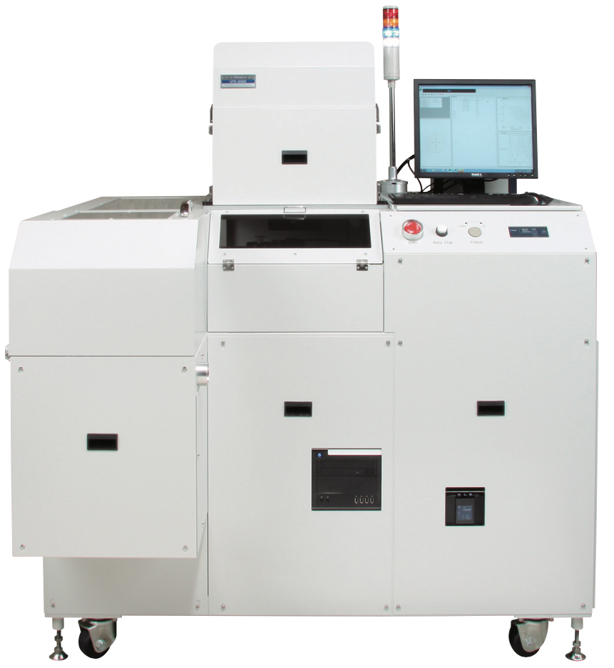
Jasco UTS-200 film thickness measurement system
Semiconductor/FPD solutions
The thickness of the opitaxial layer, substrate, etching (residual layer), liquid crystal cell gap and other semiconductor layers dramatically impacts semiconductor device performance. Management of layer thickness during the manufacturing process is extremely crucial for production of large yields of stable devices.
Jasco’s film thickness measurement system is a non-destructive, non-contact analysis method using the latest interferometric technology to provide rapid film thickness measurements. Utilizing a proprietary frequency analysis method, the sample interference spectrum is converted to a spatialgram and the film thickness calculated with a high degree of accuracy. This integrated system offers the film thickness measurements required for the exacting standards of the semiconductor industry including high-speed sample mapping; a wide thickness measurement range; and a refined operating environment, supporting a wide range of analysis requirements from process use to R&D. Jasco offers near-infrared and mid-infrared models according to the thickness measurements desired.